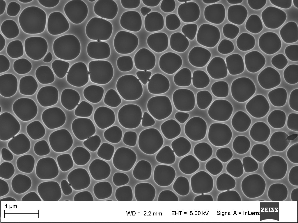
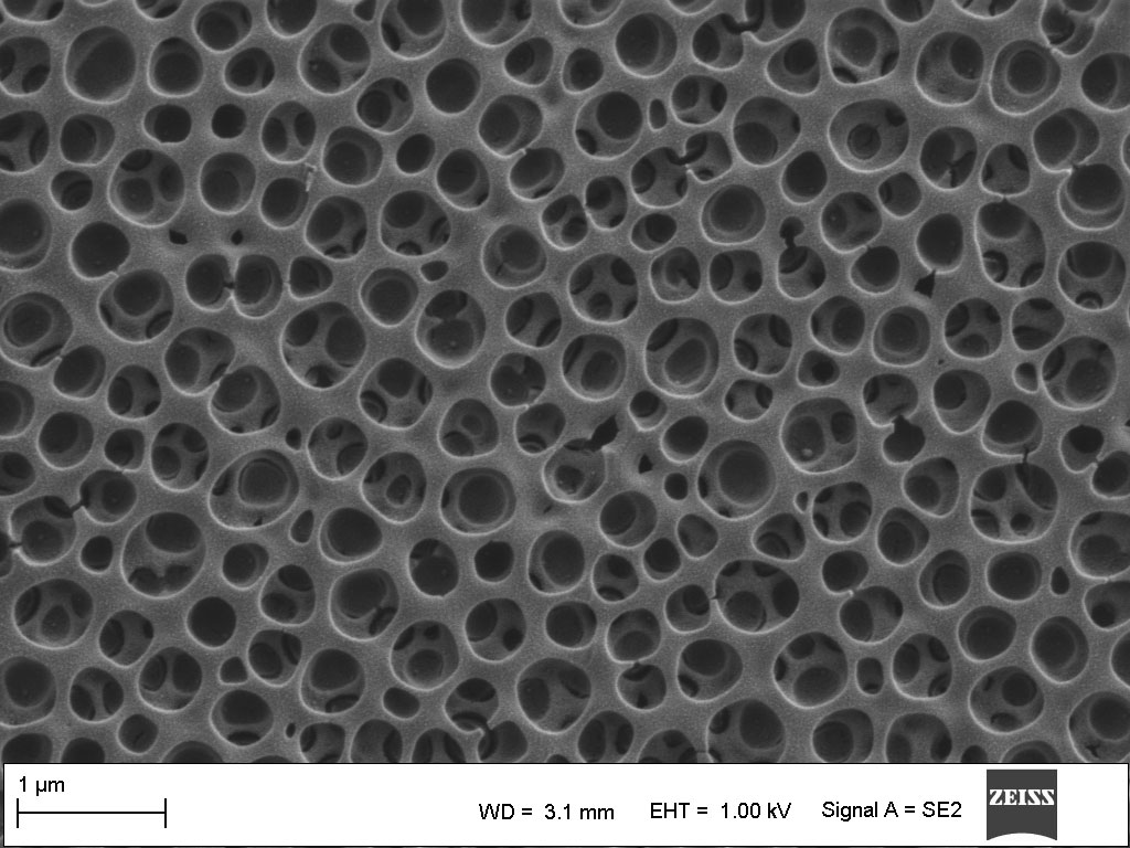
In addition to electrochemical pattterning of metals ,a chemical process that allows patterning of metal and polymer surfaces has been developed at IMST. Using a proprietary sol-gel route (porous layers and processing thereof, DE 102010044234), metal and polymer surfaces can be patterned using exogeneous oxides or polymer layers. Oxide layers of titanium, silicon, tantalum and zinc can be processed with a tailorable morphology depending on the precursor solution chemistry. An example of titanium oxide (TiO2) layers with ordered pores that were processed on a stainless- steel substrate is shown in the figure below.
Titanium oxide layers with ordered pore structures on a stainless- steel substrate. Left: a thin layer; right a thicker layer.
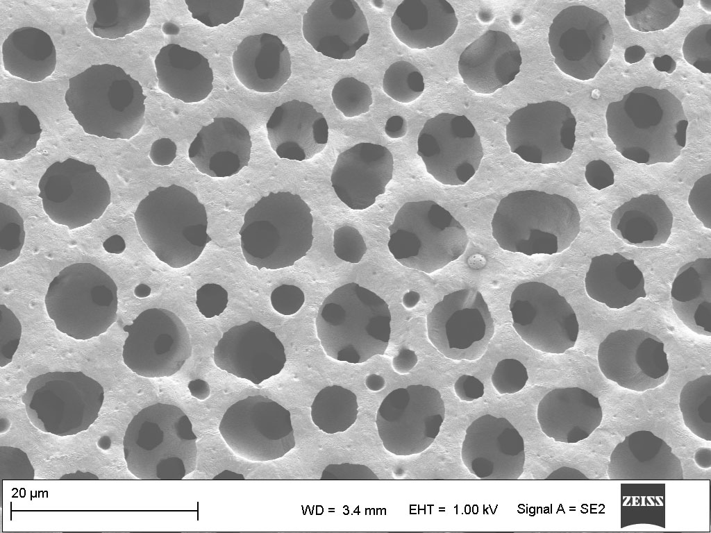
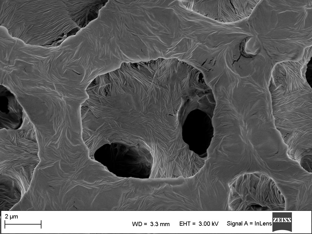
In a similar process to that used for oxides, polymer layers can also be processed on various substrates. The figure below shows a layer of Polyvinylidenfluoride (PVDF, a well-known structural and functional polymer) on a steel substrate. The pore size may be varied between 1 and 10 µm and the layer thickness between 1 and 100 µm. Self-standing membranes can also be processed using the same process.
A porous PVDF layer on a steel substrate, left at low, right at higher magnification